Selected Publications
1. p-type transparent superconductivity in a layered oxide
T. Soma, K. Yoshimatsu, & A. Ohtomo
Science Advances 6, eabb8570 (6 pages) (2020).
 Two-dimensional layered oxides can realize all
Just as you look at your smartphone every day, the transparent conductors on your smartphone look at you every day. Transparency and conductivity are always balanced, and additional weight often leads to imbalances. We found that high transparency do not cost for high conductivity that reaches even superconductivity at low temperatures in p-type layered niobium oxide. This finding was brought about by a 3-step synthesis method that was originally developed to realize high-quality epitaxial thin films.
Figure: Schematic of p-type transparent superconductivity at strongly correlated two-dimensional NbO2 layer in Li1−xNbO2 epitaxial films. The samples were prepared by Takuto Soma.
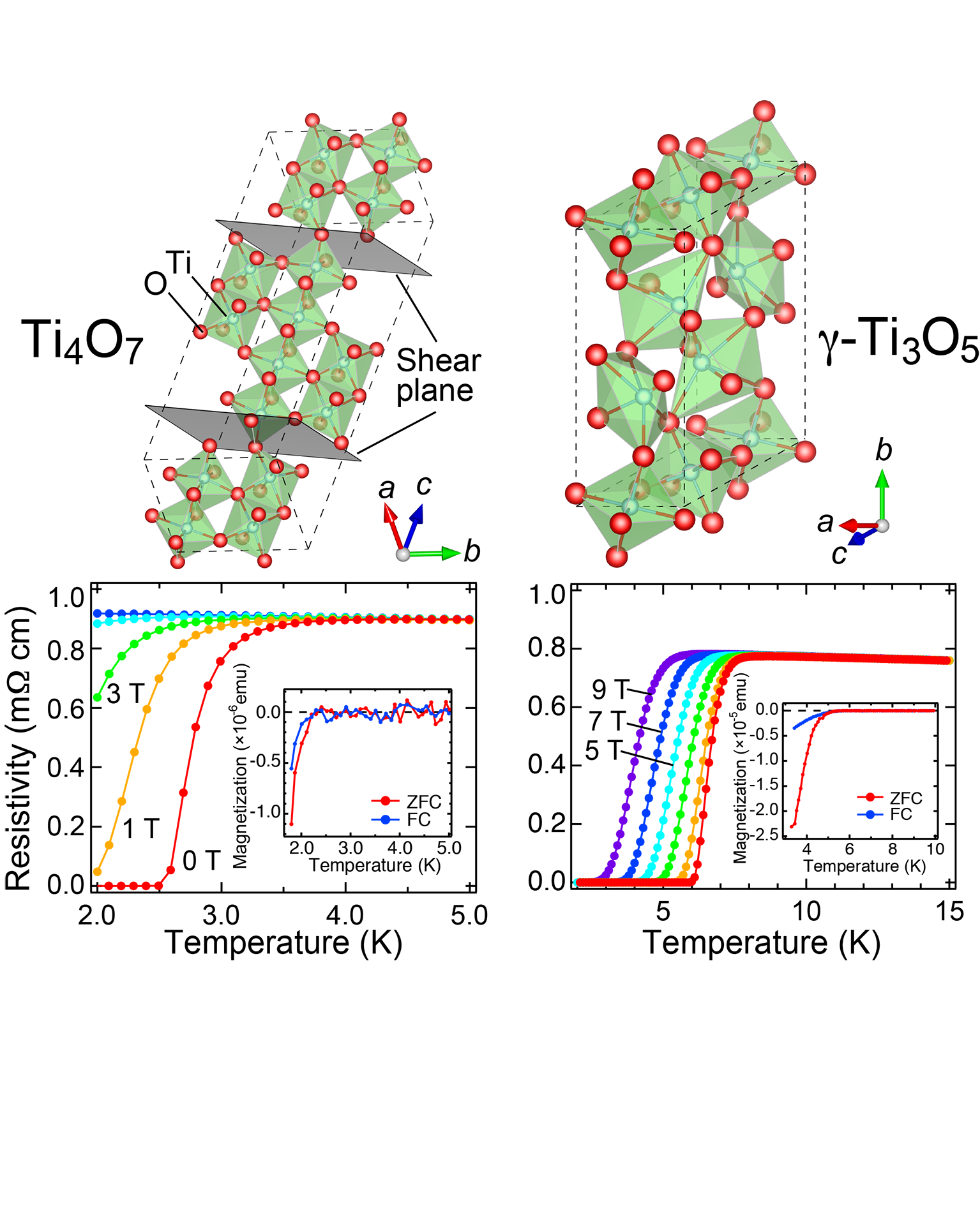
2.Superconductivity in Ti4O7 and γ-Ti3O5 films
K. Yoshimatsu, O. Sakata & A. Ohtomo
Scientific Reports 7, 12544 (5 pages) (2017).
 New twin superconductors are titanic
We discover superconductivity in thin-film forms of two different titanates that are known to exist as insulators at low temperatures when they are in bulk form. The superconducting transition temperature recorded is the highest among simple metal oxides, making these titanates useful for a harmless and inexpensive candidate for next-generation electronics.
Figure: (Top) Crystal structures of Ti4O7 and γ-Ti3O5. (Bottom) Superconductivity of Ti4O7 and γ-Ti3O5 films with the onsets of critical temperatures of 3.0 K and 7.1 K, respectively. The samples were prepared by Kohei Yoshimatsu.
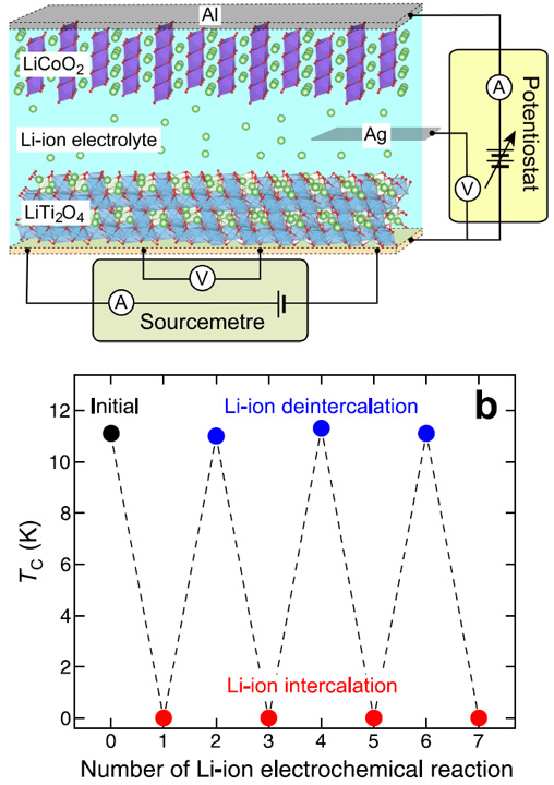
3.Reversible superconductor-insulator transition in LiTi2O4 induced by Li-ion electrochemical reaction
K. Yoshimatsu*, M. Niwa, H. Mashiko, T. Oshima & A. Ohtomo
Scientific Reports 5, 16325 (6 pages) (2015).
Vital superconductivity in a battery
Li-ion battery, an essential tool that we use every day, involves electrodes with Li ions intercalated, and an electrolyte solution that allows transport of Li ions between the electrodes for charging and discharging. Using this architecture with superconducting LiTi2O4, we demonstrate electrochemically induced superconductor-insulator transition in LiTi2O4.
Figure: (Top) A Li-ion battery structure with the superconducting LiTi2O4anode. (Bottom) Discharge and charge of the battery repeatedly switch LiTi2O4 from superconducting to insulator, and vice versa. The samples were prepared by Mifuyu Niwa (currently Asahi Kasei Corporation, Japan).
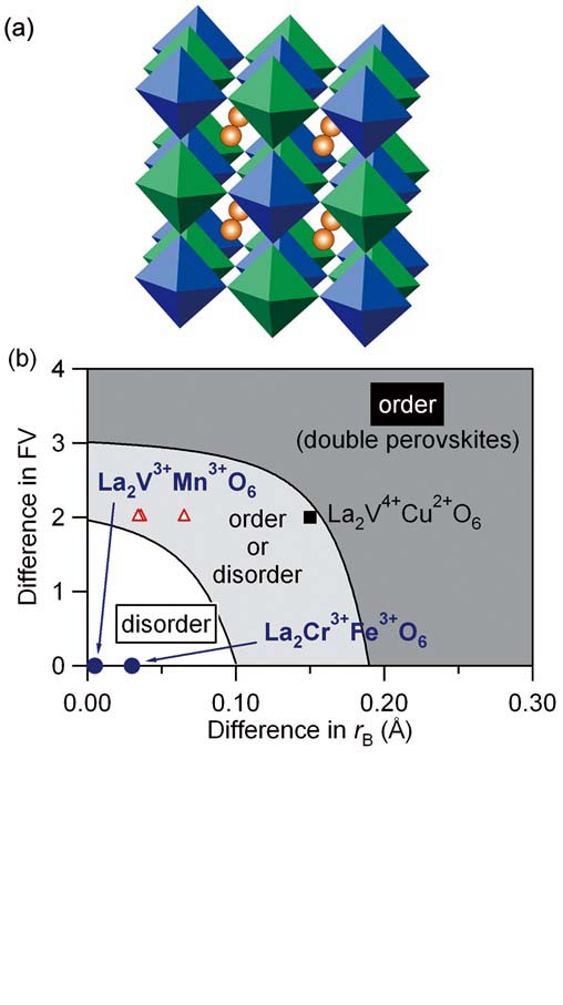
4.Spontaneous atomic ordering and magnetism in epitaxially stabilized double perovskites
A. Ohtomo*, S. Chakraverty, H. Mashiko, T. Oshima & M. Kawasaki*
Journal of Materials Research 28, 689-695 (2013).
Everything goes from disorder to order
Although double-perovskite oxides are an exotic class of magnetic materials exhibiting high-Tc ferromagnetism, synthesis of well-ordered compounds is limited to a range of B-site cation combination. Using pulsed-laser deposition technique, we find a facile synthesis route even for the combinations with vanishingly small differences in formal valence and ionic radii, La2VMnO6 and La2CrFeO6, for example. This enables us to explore new spin ordering systems in almost everything that are previously known as single perovskites (disorder).
Figure: (Top) Schematic unit lattice of double-perovskite A2B′B″O6. The transition metals B′ and B″ surrounded with six-coordinated oxygen ions form a rock-salt-type sublattice. (Bottom) Bulk phase diagram as a function of differences in formal valence (FV) and ionic radii (rB). Three double-perovskite oxides highlighted by labels were synthesized by Suvankar Chakraverty (currently INST, India)
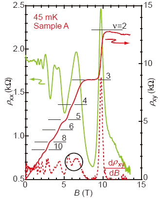
5.Observation of the fractional quantum Hall effect in an oxide
A. Tsukazaki*, S. Akasaka, K. Nakahara, Y. Ohno, H. Ohno, D. Maryenko, A. Ohtomo & M. Kawasaki*
Nature Materials 9, 889-893 (2010).
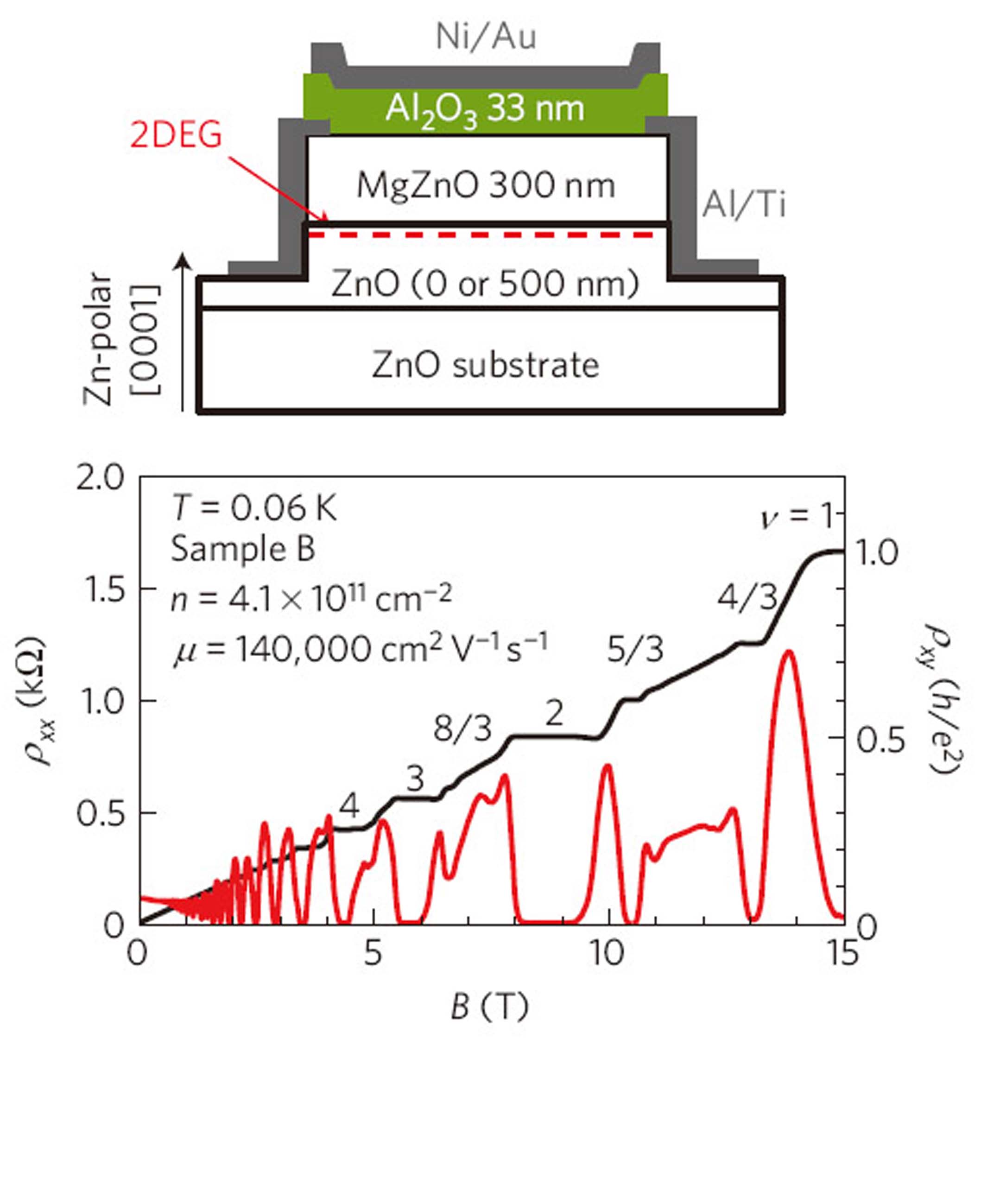
The world’s cleanest oxide
Fractional quantum Hall effect (FQHE) is a physical phenomenon that happens only in exceptionally pure semiconductor materials. This level of material purity is no longer measurable by using any chemical analysis. ZnO becomes the first oxide member of a class of materials exhibiting FQHE.
Figure: (Top) Schematic cross-section of a MBE-grown ZnO heterostructure. The two-dimensional electron gas (2DEG) is located near the interface. (Bottom) FQHE. The sample was prepared by Atsushi Tsukazaki (currently Tohoku Univ.) and colleagues at Rohm Co., Ltd. Japan.
6.Nitrogen doped MgxZn1-xO/ZnO single heterostructure ultraviolet light-emitting diodes on ZnO substrates
K. Nakahara*, S. Akasaka, H. Yuji, K. Tamura, T. Fujii, Y. Nishimoto, D. Takamizu, A. Sasaki, T. Tanabe, H. Amaike, T. Onuma, S. F. Chichibu, A. Tsukazaki, A. Ohtomo & M. Kawasaki*
Applied Physics Letters 97, 013501 (3 pages) (2010).
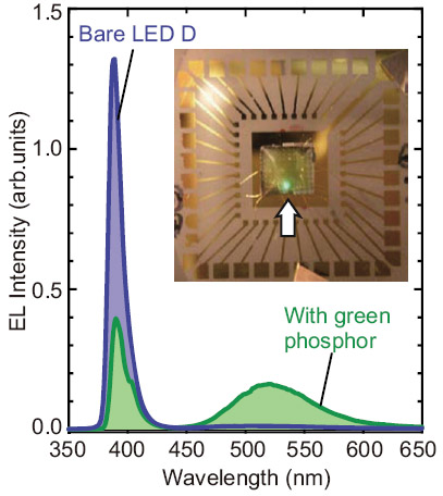
Environmentally benign solid state lighting
The use of ammonia gas with MBE technique for doping nitrogen into homoepitaxial MgZnO layer improved brightness of UV LED more than 10,000 times greater than one we made before. This process will be useful for low-cost production of white LED.
Figure: Room-temperature electroluminescence spectra for bare and green-phosphor-coated diode operated at 40 mA. Inset is a picture taken under standard laboratory illumination. The sample was prepared by Ken Nakahara and his team at Rohm Co., Ltd. Japan and Tohoku University.
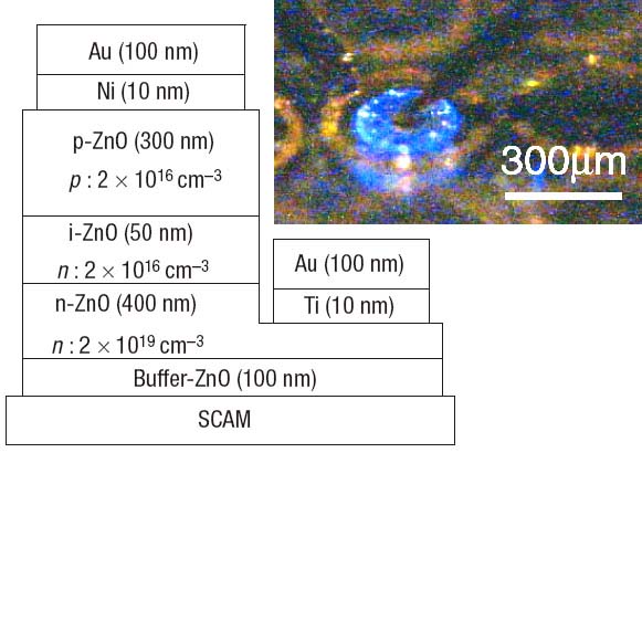
7.Electronic-field control of two-dimensional electrons in polymer-gated-oxide semiconductor heterostructures
M. Nakano, A. Tsukazaki, A. Ohtomo, K. Ueno, S. Akasaka, H. Yuji, K. Nakahara, T. Fukumura & M. Kawasaki*
Advanced Materials 22, 876-879 (2010).
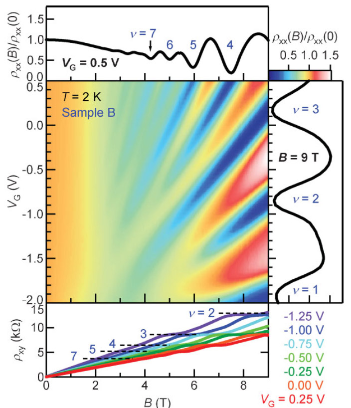 Transparent polymer gate for oxide transistors
A conducting polymer Schottky gate made of spin-coated PEDOT:PSS presents promising possibility for making low-cost, easy-to-make, and high-performance oxide devices such as transparent high-electron mobility transistors and high-efficiency UV phototransistor.
Figure: Magnetoresistance of 2DEG in a ZnO heterostructure at various gate voltage. The data clearly demonstrate the integer quantum Hall effect. Mobility was ~ 20,000 cm2/Vs. The sample was prepared by Masaki Nakano (currently Univ. Tokyo) and colleagues at Rohm Co., Ltd. Japan and Tohoku University.
8.Electric-field-induced superconductivity in an insulator
K. Ueno*, S. Nakamura, H. Shimotani, A. Ohtomo, K. Kimura, T. Nojima, H. Aoki, Y. Iwasa & M. Kawasaki*
Nature Materials 7, 855-858 (2008).
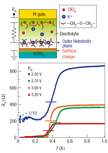
Turning an insulator into a superconductor without doping
A new way is developed for realizing superconducting materials that is expected to explore energy saving and environmentally benign society.
Figure: (Top) Schematic diagram of an electric double layer formed at an electrolyte-SrTiO3 interface. Cations in the electrolyte are solvated by polyethylene oxide molecules and are electrostatically adsorbed on the SrTiO3 surface on application of a positive gate bias to the Pt electrode, forming an outer Helmholtz plane with positive charge. (Bottom) Temperature dependence of resistivity measured at various gate voltages. The sample was prepared by Kazunori Ueno (currently Univ. Tokyo).
9.Quantum Hall-effect of polar oxide heterostructures
A. Tsukazaki, A. Ohtomo*, T. Kita, Y. Ohno, H. Ohno & M. Kawasaki*Science, 315. 1388-1391 (2007).
K. Ueno*, S. Nakamura, H. Shimotani, A. Ohtomo, K. Kimura, T. Nojima, H. Aoki, Y. Iwasa & M. Kawasaki*
Nature Materials 7, 855-858 (2008).
The world’s first QHE in oxide
When two polar surfaces having different charge density are “epitaxially” connected, excess interface charge attracts a counter part of charge carriers, making two-dimensional conducting sheet. Our ability to grow low-defect materials enable to observe the first QHE in such a polar oxide heterostructure.
Figure:QHE measured for a PLD-grown ZnO/MgZnO heterostructure at low temperature. Mobility was ~ 5,000 cm2/Vs. The sample was prepared by Atsushi Tsukazaki (currently Tohoku Univ.).
10.Repeated temperature modulation epitaxy for p-type doping and light-emitting diode based on ZnO
A. Tsukazaki, A. Ohtomo, T. Onuma, M. Ohtani, T. Makino, M. Sumiya, K. Ohtani, S. F. Chichibu, S. Fuke, Y. Segawa, H. Ohno, H. Koinuma & M. Kawasaki*Nature Materials 4, 42-46 (2005).
 Beautiful UV light finally came out
ZnO is known to be an efficient UV light emitting material. But, the absence of a reproducible growth technique of p-type ZnO had prevented us from making a diode. A new growth technique is proposed to solve this long-standing issue.
Figure: The structure of ZnO homoepitaxial p-i-n junction. Inset is a picture of device operated at 5 mA. The sample was prepared by Atsushi Tsukazaki (currently Tohoku Univ.).
T. I. Suzuki, A. Ohtomo*, A. Tsukazaki, F. Satoh, J. Nishii, H. Ohno & M. KawasakiAdvanced Materials 16, 1887-1890 (2004).
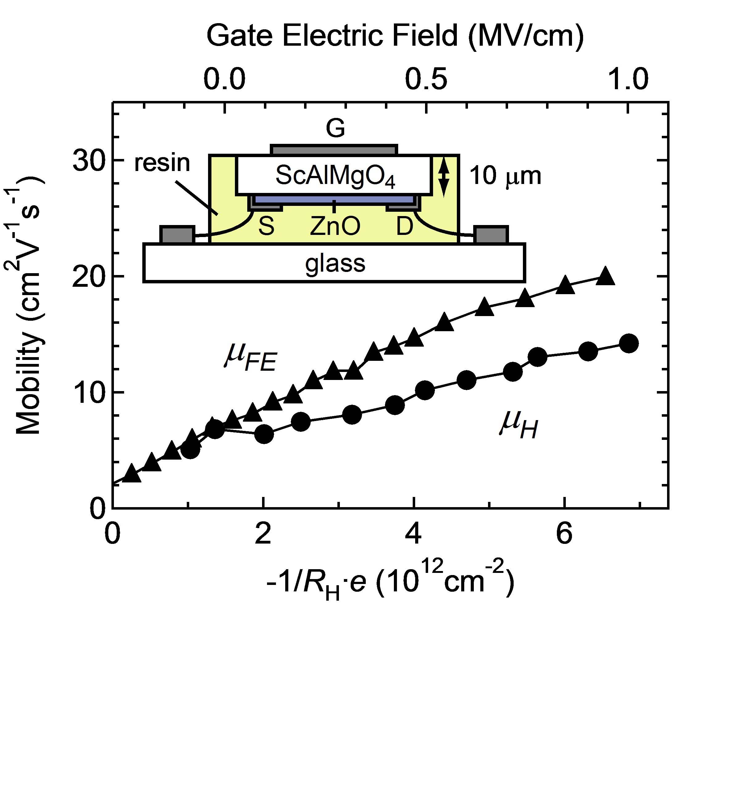 A hand-made transistor reveals a problem of practical ones
One of the advantages of ZnO transistor is that it can be fabricated at low temperature on a glass substrate or a polymer substrate. However, its mobility and long-term reliability is suppressed by the presence of dense grain boundaries network in a polycrystalline channel. Compared with the performance of a model device with a single crystal channel, the effect of grain boundaries has been unveiled.
Figure: Field-effect and Hall mobility as a function of sheet carrier density. Inset is schematic structure of the device prepared by Takao Suzuki (currently Tokyo Denpa).
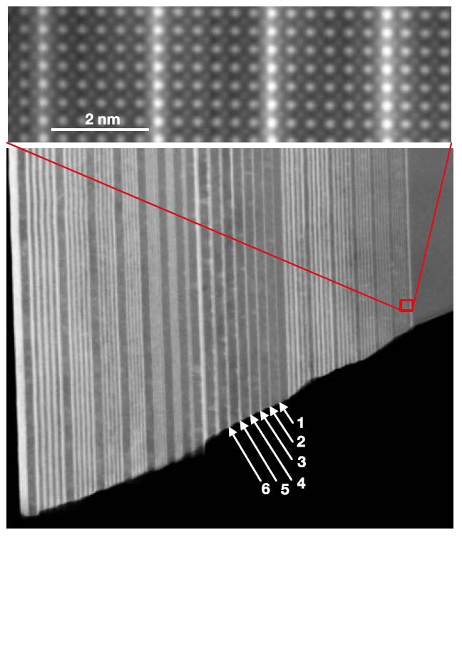
12.Atomic-scale imaging of nanoengineered oxygen vacancy profiles in SrTiO3
D. A. Muller*, N. Nakagawa, A. Ohtomo, J. L. Grazul & H. Y. HwangNature 430, 657-661 (2004).

Oxygen vacancy bubbles frozen in nanospace
At the heart to modern oxide chemistry lies the recognition that beneficial materials properties can be obtained by deliberate deviations of oxygen atom occupancy from the ideal stoichiometry. Using a PLD technique, a SrTiO3 superlattice film with oxygen doping profiles that exhibit subnanometer abruptness was fabricated.
Figure: Low-angle annular dark field image of an oxygen-modulated SrTiO3superlattice. The sample was prepared by Naoyuki Nakagawa (currently Toshiba Cooperation) and colleagues at Bell labs.
13.A high mobility electron gas at the LaAlO3/SrTiO3 heterointerface
A. Ohtomo & H. Y. Hwang*Nature 427, 423-426 (2004).
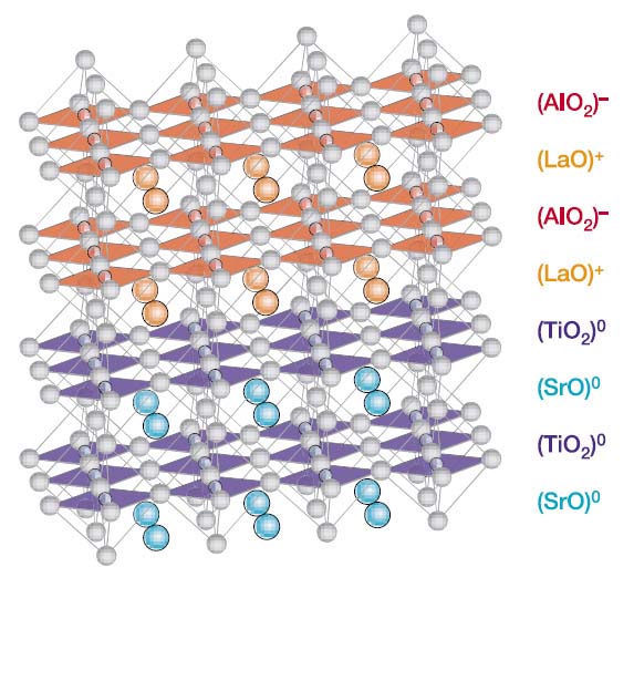
Metallic interface between insulators
Polarity discontinuities at the interfaces between different crystalline materials can lead to nontrivial local atomic and electronic structure that are inaccessible in bulk materials. A metallic interface between two insulating oxides exhibiting quantized magnetotransport has been discovered.
Figure:Schematic structure of the LaAlO3/SrTiO3 interface showing the composition and the ionic charge state of each layer. The sample was prepared by Akira Ohtomo (currently Tokyo Tech).
14.Artificial charge-modulation in atomic-scale perovskite titanate superlattices
A. Ohtomo, D. A. Muller, J. L. Grazul & H. Y. HwangNature 419, 378-380 (2002).
Pl